Hangzhou Xuhong Technology Co.,Ltd
EN
中文
The TFT LCD process is divided into array process, boxing process and module process in the sequence of processing. In this article, we will introduce the array process in detail.
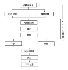
The array process is similar to the process of semiconductor technology to make patterns such as TFT devices, pixels and other pattern on the glass substrate. The array process includes cleaning technology, CVD film technology, sputter film formation technology, photoresal or optical resistance coating , development and peeling technology, exposure technology, wet carvings, dry carvings, etc.Eventually, a 4 or 5 layer of film pattern is formed on the glass substrate. The formation process of the pattern of each layer of thin film is shown in the figure:

First clean the glass substrate, and then form the film (metal use sputter, non -metal use CVD method); paint PR on the substrate after the film formation, and expose it with MASK, transfer the required patterns from MASK to PR, After being washed away from the lighting part of the PR, the PR left is the required pattern; then the etching engineering (general metal uses wet carvings, non -metal uses dry carvings), remove the PR -free film, and leave it is the left is. The required film pattern; finally peel off the PR. At the end of the array process, annealing is required, and the inspection project runs through the entire array process as required.
AUO LCD:https://www.auo-lcd.com/products/auo-lcd-screen/
Innolux lcd:https://www.auo-lcd.com/products/innolux/